In my last post, I showed you how to download Altera’s Quartus II software and get a new, empty project started for the BeMicro CV platform.
This time, we’ll learn how to build a Verilog module and compile it.
The Blank Slate
We left off looking at a blank slate, an empty project.
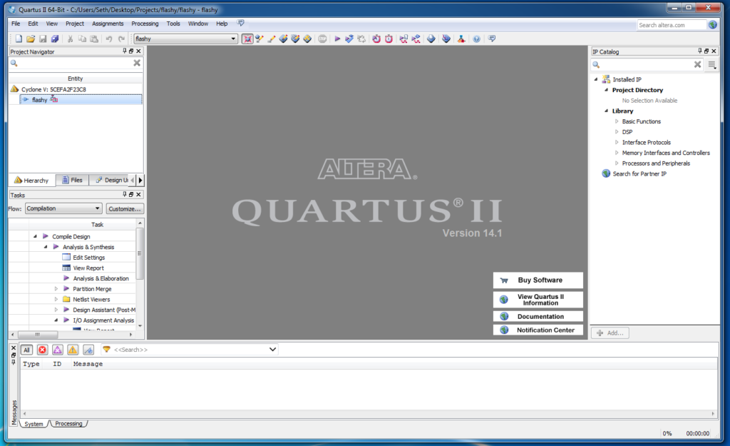
This is always the most intimidating part of any project. What do we want to do?
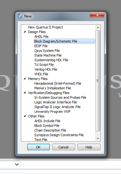
The next step is to define a top-level design file. From the menu. select File ? New…, and you will be presented with a list of components. Select Block Diagram/Schematic File from the list.
Next, click File ? Save As… from the menu, and save the new top level design file as flashy.bdf.
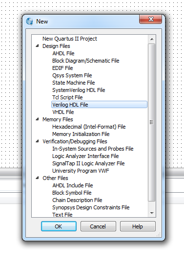
We won’t get very far with just a blank design file. We need a Verilog Module to define the behavior we want from our counter, so next, choose File ? New… from the menu, and select Verilog HDL File. This will open up a blank Verilog file, ready for your input.
The Verilog “counter.v” Module
Verilog is a language that defines how our FPGA is to behave. It’s tempting to think of it as a programming language, but it’s dangerous to fall into this trap. It’s not a programming language, it’s a hardware definition language.
What’s the difference? A programming language describes linear process that implements an algorithm step-by-step. A hardware definition language, on the other hand, describes how a digital circuit should behave using words. It is not implementing an algorithm, it’s implementing a circuit!
The distinction can seem very subtle. When you’re describing how hardware behaves, it can certainly look very much like a program or an algorithm. But it’s not, and it’s always very important to keep that in mind. So, we want to design a circuit that will take a 50 MHz clock signal as input, and count down on the 8 LED outputs forever.
Here’s our Verilog module to describe that behavior. Save this file as “counter.v”:
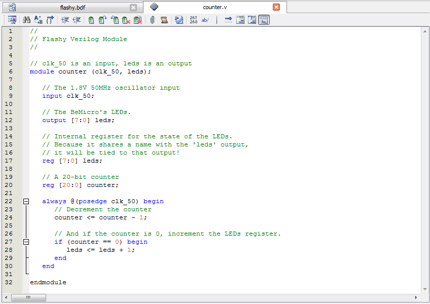
It’s short and sweet. The top-level module definition has two arguments, clk_50, which we will map to our 50 MHz clock signal, and leds, which we will map to our LED outputs.
Internally, there are two registers: an 8-bit register named leds, and a 21-bit register named counter. These are used to latch state in the circuit. Because we’ve named one of the registers the same as one of the outputs, they will be automatically connected for us.
The critical part of the circuit description is the always @(posedge clk_50) block. This describes what happens at the positive edge of a clock trigger on the clk_50 input. It says that we decrement our counter register, and if the counter happens to be all 0’s, we latch the state of the LEDs plus one into the leds register. We’re using the internal counter register as a delay to slow down the rate at which we update the LEDs.
You may be confused at this point, because I said our circuit was going to count down, but clearly we’re incrementing the leds register. What’s that about? Well, it turns out the BeMicro CV uses LEDs that are active low, meaning that they light up when the corresponding output is grounded. The end effect is that if you want all the outputs lit, you write 00000000 to the output. In other words, when we count up with our leds register, it looks like the LEDs are counting down. If you wanted the LEDs to count up, you could just invert the output. I’ll leave that as an exercise to the reader.
Adding the Verilog Module to the Project
We’ve described a simple circuit here. Now we need to tell Quartus how to connect the inputs and outputs of our circuit. To do that, we’ll first need to make a circuit diagram symbol for our module.
Right-click on the “counter.v” file in our project, and select Create Symbol Files for Current File
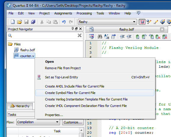
Quartus should compile your file. If you get any errors, double-check to make sure there are no typos! After it’s compiled, you can close the Compilation Report tab, and then return to the flashy.bdf tab.
Right-click anywhere inside the flashy.bdf tab, and select Insert ? Symbol… from the context menu.
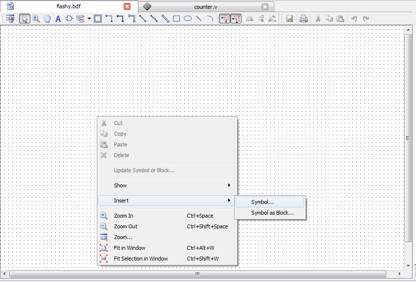
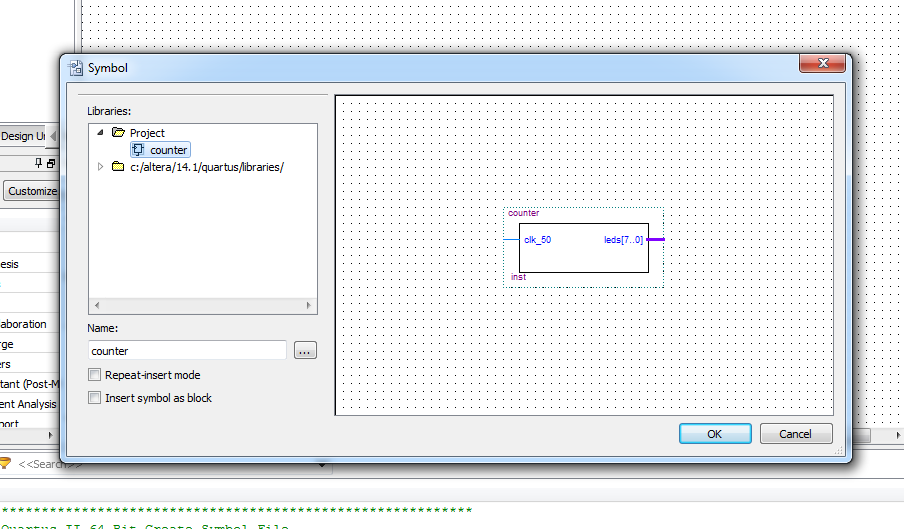
You should be presented with a dialog like this. Select the counter symbol from the Project folder, click OK, and then drop the symbol anywhere into the flashy.bdf tab.
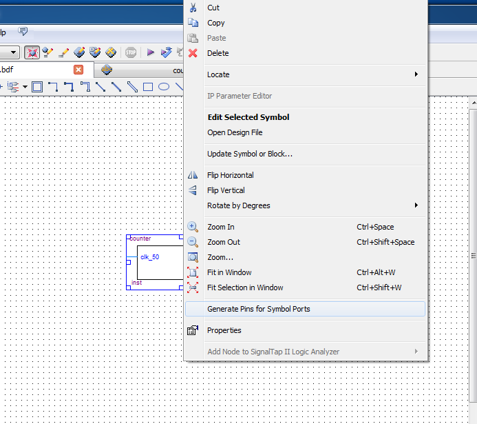
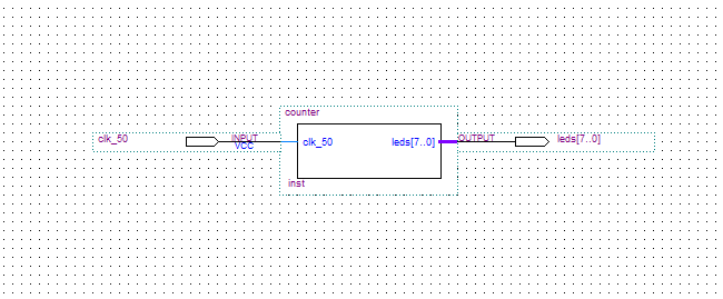
Now we have a symbol placed into our project, but we still need to map its inputs and outputs. Right-click on the symbol you’ve just placed, and select Generate Pins for Symbol Ports from the menu.
There, now things look a little more complete. We can see that we have some pins named clk_50 and leds[7..0].
Connecting The Pins
Although our symbol now has inputs and outputs, those inputs and outputs are not yet connected to the real physical BeMicro hardware! To do that, we’ll need Quartus’s help.
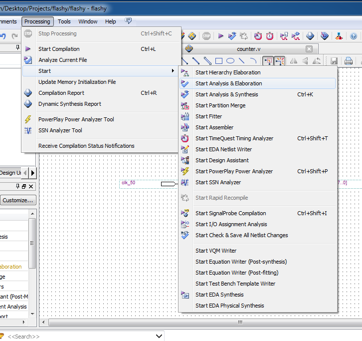
From the menu, select Processing -> Start -> Start Analysis & Elaboration. This step will analyze our top-level schematic and figure out how many inputs and outputs we’ll actually be using on our FPGA chip.
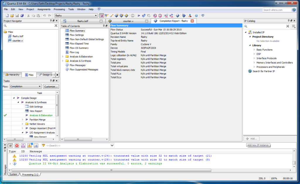
The module will compile, and Quartus will analyze it. Depending on your hardware, this may take a minute or two. You should eventually see a compilation report letting you know the analysis was successful. You can close the compilation report once you’re done reviewing it.
Now comes the critical part: We can map our circuit’s inputs and outputs to real FPGA pins!
From the Assignments menu, select Pin Planner
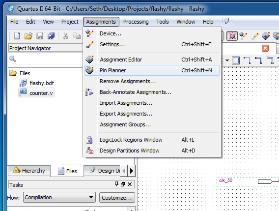
You should be presented with the Pin Planner. This dialog allows you to map the flashy inputs and outputs to the FPGA’s pins. You’re actually looking at a real map of all 484 pins on the FPGA, but don’t worry — we’re only going to be using nine of them!
This is where we have to turn to the BeMicro’s documentation for help. We want to figure out what input the 50 MHz clock is on, and what outputs the LEDs are on. I’ll save you some time and pain by just putting the information here, because it turns out that the BeMicro CV documentation is wrong. Their mapping of LED pins is out of order. Oops!
Here’s how the BeMicro CV actually maps its pins:
| FPGA Pin | Voltage | BeMicro Mapping |
|---|---|---|
| H13 | 1.8V | 50 MHz Clock |
| Y3 | 3.3V LVCMOS | LED 7 |
| AA2 | 3.3V LVCMOS | LED 6 |
| AA1 | 3.3V LVCMOS | LED 5 |
| W2 | 3.3V LVCMOS | LED 4 |
| U2 | 3.3V LVCMOS | LED 3 |
| U1 | 3.3V LVCMOS | LED 2 |
| N2 | 3.3V LVCMOS | LED 1 |
| N1 | 3.3V LVCMOS | LED 0 |
We need to map these using the Pin Planner. In the end, your Pin Planner should look like this:
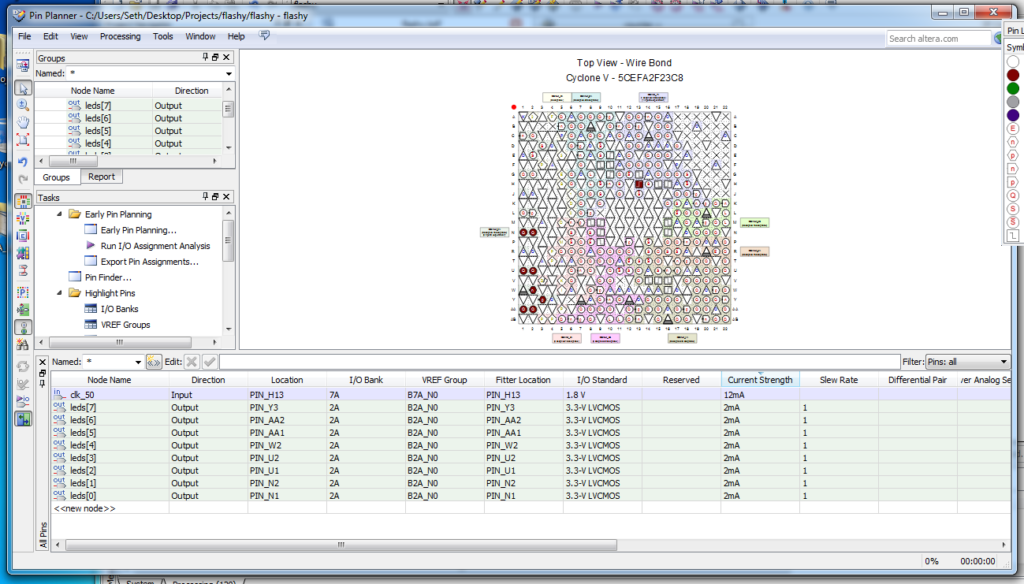
It’s safe to close the Pin Planner window now, and you’ll notice that the symbol has changed somewhat, to show that the inputs and outputs have been mapped.

Now you’re ready to compile the whole project. From the Processing menu, select Start Compilation. Compiling should take a minute or two, depending on your hardware.
Once it’s all done, congratulations! You’ve built your first FPGA module! Now all you need to do is actually load it onto the FPGA and start it running. We’ll cover that in our next and final blog installment.
Comments