Table of Contents
- Introduction
- Bibliography
- System Board
- Expansion Cards
- Interrupts
- Miscellaneous Notes
- Appendix A: System Board Components
Introduction and Overview
The purpose of this page is to document the internals of the AT&T 3B2 Revision 2 line of computers, specifically the AT&T 3B2/310 and AT&T 3B2/400. It started in 2015 as a set of notes that I kept for myself while trying to reverse engineer the 3B2/400. Since then, I’ve managed to track down additional documentation and resources that have helped expand my understanding quite a bit.
Nevertheless, here is still scant information online about the internals of the 3B2. It has proven very difficult to find detailed documentation about how the 3B2 actually works. This page attempts to address that by collecting what I have learned into one place.
But why the 3B2? In large part because it is historically significant, and yet not very well known. The 3B2 was AT&T’s main porting platform for System V Release 3 UNIX™ (SVR3). It is a fully 32-bit computer system built around a microprocessor and chipset by Western Electric called the WE32100. The WE32100 and its earlier predecessor, the WE32000 (collectivey known as BELLMAC-32 processors), represented major leaps forward in building architectures specially suited for UNIX.
Bibliography
In addition to lots of probing of a 3B2/400 system board with an oscilloscope and a logic analyzer, the following documents have been invaluable in this work.
- The WE 32100 Microprocessor Information Manaual, Document number 451-000, AT&T, 1985
- WE 32-Bit Microprocessors and Peripherals Databook, A&T, 1987
- AT&T 3B2 Computer Technical Reference Manual, Document number 305-490, AT&T, 1990
- Hardware Configurations and I/O Protocol of the WE32100 Microprocessor Chipset, M. L. Fuccio, L. G. Goyal, B. Ng, AT&T Bell Laboratories
- Hardware Architecture Considerations in the WE32100 Chip Set, M. L. Fuccio, B. Ng, AT&T, “IEEE Micro”, April 1986
- 3B™2 Component Requirements and Specifications: I/O Bus, Internal Memo, P.M. Walsh, AT&T, 1983
- 3B™2 Circuit Description: Common I/O Hardware, Issue 1, Internal Memo, P.M. Walsh, AT&T, 1983
- AT&T 3B2 and 3B5 Computer Driver Design Guide, Document number 305-495, AT&T, 1984
- AT&T UNIX System V Release 3 Source Code, AT&T, 1985-1988
- AT&T 3B2 ROM Images (Link to GitHub)
- Disassembled Model 400 ROM image (Link to GitHub)
- “The Design of the UNIX Operating System”, Maurice J. Bach, 1986
System Board
Major Components
The 3B2/400 amd 3B2/310 share the same system board. The major parts of the architecture include:
- WE32100 CPU
- WE32101 MMU
- WE32102 Bi-phase Crystal Oscillator
- WE32106 Math Accelerator Unit (Optional)
- 4 x D2764A EPROMs holding the system boot ROM
- TMS2797NL floppy disk controller
- NEC μPD7261A hard disk controller
- NEC μPD8253C interval timer
- AM9517A Multimode DMA Controller
- SCN2681A Dual UART
- MM58174A Real Time/Time of Day clock
In addition to these major components, there is a tremendous amount of LSI glue logic, plus 14 PLAs/PALs on the system board. These implement the DRAM controller, Control Status Register, and Interrupt Logic. Their exact layout is unknown, as no schematics are available, however the system board block diagram below helps document the over-all architecture at a high level.
Finally, there is one 18-pin DIP package IC labeled with in-house part number “O WE 62C”, stamped with a date code and the number “53”. The chip remains unidentified. Presumably it is custom LSI logic.

Memory Map
ROM Space
The ROM is mapped too the bottom 64KB of the address space, at physical
addresses 0x00000000 – 0x0000ffff. The ROM itself is only 32KB,
so I still need to do some additional diagnostic programming to determine
exactly how the ROM maps to the top half of its space, if at all.
When running under SVR3, the ROM is mapped at virtual address
0x00020000.
I have decoded and disassembled the ROM, and discovered that there are several distinct areas
- Strings
- Vector Tables
- Code
- System Version Number
The Vector Tables are described in detail in the SVR3 source code, in the
header file sys/firmware.h.
Special RAM Locations
| ROM | Pointer | SVR3 Name | Description |
|---|---|---|---|
0x48c | 0x02000864 | p_runflag | Flag indicating whether system is safe for booting |
0x490 | 0x02001514 | p_edt | Ptr to Equipped Device Table (EDT) |
0x494 | 0x020011f8 | p_inthand | Ptr to location containing address of interrupt handlers |
0x498 | 0x020011f4 | p_exchand | Ptr. to location containing address of exception handler |
0x49c | 0x02000858 | p_rsthand | Ptr. to location containing address of reset handler |
0x4a0 | 0x02001200 | p_cmdqueue | Ptr. to command queue for boot command |
0x4a4 | 0x020012a8 | p_fl_cons | Ptr. to float cons struct |
0x4a8 | 0x0200126c | p_option | Ptr. to Ptr. to Option Number (for getedt) |
0x4c4 | 0x02001268 | p_access | Access permissions for printf, etc. |
0x4e0 | 0x020011f0 | p_num_edt | Ptr. to location containing number of devices in EDT |
0x4e4 | 0x020011ec | p_memsize | Ptr. to location containing size of main memory |
0x4e8 | 0x02001504 | p_memstart | Ptr. to location containing start of main memory for UNIX |
0x4f0 | 0x02000a80 | p_physinfo | Ptr. to disk physical info |
0x4f4 | 0x02001258 | p_pswstore | Ptr. to PSW before exception or interrupt |
0x4f8 | 0x0200125c | p_pcstore | Ptr. to PC before exception or interrupt |
0x4fc | 0x020011e8 | p_console | Ptr. to pointer to console UART |
0x504 | 0x02001264 | p_save_0 | Ptr. to %r0 before exception |
0x50c | 0x020012d8 | p_bpthand | Ptr. to location containing address of exception handler |
0x510 | 0x020012d0 | p_spwrinh | Location for soft power inhibit |
0x514 | 0x0200086c | p_meminit | Location for memory init flag |
0x52c | 0x020012dc | dmn_vexc | Demon virtual process / stack exception handler PCB |
0x530 | 0x020012e0 | dmn_vgate | Demon virtual gate table location |
0x534 | 0x020012e4 | dmn_vsint | Demon virtual stray interrupt PCB location |
0x544 | 0x02000a74 | p_hdcspec | Location of fw hdc spec params |
ROM Routines
| ROM | Pointer | Name | Description |
|---|---|---|---|
0x4ac | 0x00004dd4 | p_getedt | Routine to fill EDT structure |
0x4b0 | 0x000044e4 | p_printf | Location of printf routine |
0x4b4 | 0x00004360 | p_gets | Location of gets routine |
0x4b8 | 0x00004ae4 | p_sscanf | Location of sscanf routine |
0x4bc | 0x00007f68 | p_strcmp | Location of strcmp routine |
0x4c0 | 0x00002af8 | p_excret | Routine to set up a return point for exceptions |
0x4c8 | 0x00004484 | p_getstat | Routine to check console for a character present |
0x4cc | 0x00005320 | p_chknvram | Location of routine to verify checksum over NVRAM |
0x4d0 | 0x00005224 | p_rnvram | Location of routine to read NVRAM |
0x4d4 | 0x000052a0 | p_wnvram | Location of routine to write NVRAM |
0x4d8 | 0x00007698 | p_hd_cs | Location of routine to access hard disk |
0x4dc | 0x00007b2c | p_fd_cs | Location of routine to access floppy disk |
0x4ec | 0x00001168 | p_release | Pointer to location containing release of code |
0x500 | 0x00003d74 | p_setbaud | Pointer to setbaud routine |
0x508 | 0x00007ff0 | p_serno | Pointer to serial number struct |
0x518 | 0x00005438 | p_bzero | Pointer to memory zero routine |
0x51c | 0x00005450 | p_setjmp | Pointer to setjmp routine |
0x520 | 0x000054a1 | p_longjmp | Pointer to longjmp routine |
0x524 | 0x00004e14 | p_dispedt | Pointer to display edt routine |
0x528 | 0x00005504 | p_hwcntr | pointer to DUART counter delay routine |
0x538 | 0x000055ec | p_fw_sysgen | Pointer to generic sysgen routine |
0x53c | 0x00005baa | p_ioblk_acs | Pointer to ioblk_acs routine |
0x540 | 0x000051d2 | p_brkinh | Pointer to break inhibit routine |
0x548 | 0x0081e100 | p_symtell | Function to tell xmcp where the symbol table is |
0x54c | 0x0000421f | p_demon | Function to enter demon without init |
String Locations
There’s a large block of string literals in the ROM which are referenced by the various subroutines. I have added these to the ROM source code as I’ve found them.
IO Space
Looking through the SVR3 source code has revealed the following system
board map, in the file usr/src/uts/3b2/vuifile.
| Name | Address | Description |
|---|---|---|
unxsbdst | 0x40000 | System Board Start Address |
mmusdc1 | 0x40000 | MMU SDC bits 0-31 |
mmusdc2 | 0x40100 | MMU SDC bits 32-64 |
mmupdc1r | 0x40200 | MMU Right Half PDC Bits 0-31 |
mmupdc2r | 0x40300 | MMU Right Half PDC Bits 32-63 |
mmupdc1l | 0x40400 | MMU Left Half PDC Bits 0-31 |
mmupdc2l | 0x40500 | MMU Left Half PDC Bits 32-63 |
mmusrama | 0x40600 | MMU Section RAM A |
mmusramb | 0x40700 | MMU Section RAM B |
mmufltcr | 0x40800 | MMU Fault Code Register |
mmufltar | 0x40900 | MMU Fault Address Register |
mmucr | 0x40a00 | MMU Configuration Register |
mmuvar | 0x40b00 | MMU Virtual Address Register |
sbdpit | 0x42000 | Programmable interval timer (8253) |
clrclkint | 0x42013 | Clear clock interrupt |
sbdnvram | 0x43000 | NVRAM (0x400 bytes) |
sbdrcsr | 0x44000 | CSR Read (reads the whole 16-bit halfword) |
sbdwcsr | 0x44000 | CSR Write base address |
dmaid | 0x45000 | DMA Integrated Disk (hard disk) page buffer |
dmaiuA | 0x46000 | DMA UART A page buffer |
dmaiuB | 0x47000 | DMA UART B page buffer |
dmac | 0x48000 | DMA controller status/command register |
duart | 0x49000 | 2681 UART |
idisk | 0x4a000 | 7261 Disk Controller |
ifloppy | 0x4d000 | 2797 Floppy Controller |
dmaif | 0x4e000 | DMA Integrated Floppy page buffer |
RAM Space
Main memory (“mainstore”) appears to start at 0x2000000 on the 3B2.
Interestingly, on SYSVR3 this is mapped to /dev/mainstore.
WE32100 CPU
As stated, the CPU is the WE32100 32-bit CPU. It has both a 32-bit address bus and a 32-bit data bus. The CPU has 9 general purpose and 7 special purpose 32-bit registers, supports four privilege modes (User, Supervisor, Executive, Kernel), supports addressing in words (32-bit), halfwords (16-bit), and bytes (8-bit), and has a highly orthogonal instruction set with many addressing modes. It is paired with the WE32101 MMU, the WE32102 dual-phase crystal oscillator which provides two 10MHz clocks 90° out of phase, and the optional WE32106 Math Accelerator UNIT.
WE32101 MMU
The WE32101 MMU provides virtual address to physical address translation using both segmented and paged memory.
On the 3B2, virtual address space is divided into four sections, identified by the top two bits of the address.
The MMU uses these top two bits as a Segment ID (SID) to look up the address in physical memory of a Segment Descriptor Table (SDT).
The next 13 bits of the address are known as the Segment Select field, and are used to index into the Segment Descriptor Table to find a Segment Descriptor.
The Segment Descriptor contains a bit that determines whether the virtual address being translated is to be treated as a Contiguous Segment, or Paged.
The rest of the bits of the virtual address are then treated differently depending on the value of this bit.
This process is described in great detail in the WE 32100 Microprocessor Information Manual and in the WE 32101 MMU datasheet.
Segmented Memory Virtual Addresses
Segmented virtual addresses further divide the virtual address into a Segment Offset (SOT). The physical memory address is then translated as in the figures below.


Paged Memory Virtual Addresses
Paged virtual addresses further divide the lower 17 bits into a 6-bit Page Select field and an 11 bit Page Offset field. The physical memory address is then translated as in the figures below.


8253 Programmable Interval Timer
This timer is responsible for driving much of the interrupt system. Its functions are IO mapped to the following addresses:
| Physical Address | 8253 Function | SBD Function |
|---|---|---|
0x42003 | Counter 0 | Sanity Timer (used for softpower) |
0x42007 | Counter 1 | Interval Timer |
0x4200b | Counter 2 | Not yet known |
0x4200f | Command | |
0x42013 | Clear Latch |
-
Counter 0: Set during ROM init. This appears mainly to be used for softpower status. The clock for Counter 0 on pin 9 runs at 100KHz.
-
Counter 1: Set during UNIX boot. Provides the level 15 interrupt used by UNIX for process switching. This is initialized to
0x03e8(decimal1000) by UNIX in the functionclkstrt(). This gives us a period of 10ms, since the clock on Counter 1 on pin 15 runs at 100KHz. -
Counter 2: Set during ROM init. The clock for Counter 2 on pin 18 runs at 2MHz. We don’t know what this is for. It’s not referenced in the AT&T source code. The ROM initialization puts
0xa(decimal 10) into the counter, so the timer output (if enabled) would pull low for 500ns every 5μs. So far, I have observed only that the gate is set so that this timer is not enabled.
Control Status Register
This is just a set of latches that can be set or cleared by writing to
various memory locations, or read as a single 16-bit value. The base
address of the CSR is at 0x44000.
Two 74LS374 Octal D-Type latches provide the 16-bit CSR.
The bits and addresses of the CSR are described in detail in Figure 3-22 of the AT&T 3B2 Computer Technical Reference Manual, on page 3-68:
| Bit | Address | Function | Description |
|---|---|---|---|
| 15 | 0x44000 | Clear | Error Timer Timeout (Bus Error) |
| 14 | 0x44004 | Clear | Memory Parity Error |
| 13 | 0x44008 | Set | System Reset Request |
| 12 | 0x4400c | Clear | Clear memory alignment trap |
| 11 | 0x44010 | Set | Diagnostic indicator (Green LED) On |
| 11 | 0x44014 | Clear | Diagnostic Indicator (Green LED) Off |
| 10 | 0x44018 | Set | Floppy Motor On |
| 10 | 0x4401c | Clear | Floppy Motor Off |
| 9 | N/A | - | Reserved |
| 8 | 0x44020 | Set | Inhibit Timers |
| 8 | 0x44024 | Clear | Allow Timers |
| 7 | 0x44028 | Set | Inhibit Faults |
| 7 | 0x4402c | Clear | Allow Faults |
| 6 | 0x42010 | Clear | Clear Periodic Timer Interrupt (INT 15) |
| 5 | 0x44038 | Set | Set PIR 8 Interrupt |
| 5 | 0x4403c | Clear | Clear PIR 8 Interrupt |
| 4 | 0x44030 | Set | Set PIR 9 Interrupt |
| 4 | 0x44034 | Clear | Clear PIR 9 Interrupt |
| 3 | N/A | Read Only | UART Interrupt |
| 2 | N/A | Read Only | Floppy Disk Interrupt |
| 1 | N/A | Read Only | DMA Interrupt |
| 0 | N/A | Read Only | I/O Board Fail |
The 16 bits of the CSR, when read, map to the following bitmasks
| Name | Mask |
|---|---|
CSRTIMO | 0x8000 |
CSRPARE | 0x4000 |
CSRRRST | 0x2000 |
CSRALGN | 0x1000 |
CSRLED | 0x0800 |
CSRFLOP | 0x0400 |
CSRITIM | 0x0100 |
CSRIFLT | 0x0080 |
CSRCLK | 0x0040 |
CSRPIR8 | 0x0020 |
CSRPIR9 | 0x0010 |
CSRUART | 0x0008 |
CSRDISK | 0x0004 |
CSRDMA | 0x0002 |
CSRIOF | 0x0001 |
2681 Dual UART
The UART provides two serial ports integrated into the main system. One is the console, the other is a secondary TTY. Additionally, the UART provides a general purpose counter/timer circuit with an interrupt output.
The UART is clocked at 230.525 KHz. Due to the 16-bit counter, the maximum delay for the UART interrupt timer is 284 ms.
Floppy Drive
The standard floppy drive (known as IF, “Integrated Floppy”) is a CDC 9429. The floppy format used is a little unusual: It is a Double-Sided, Quad Density format (DSQD) holding 720KB per diskette. The format is:
- Double sided
- 80 tracks per side
- 9 sectors per track
- 512 bytes per sector
- 3:1 interleave
- 250kbps MFM data
Winchester (MFM) Hard Disk Controller
The 3B2/310 and 3B2/400 support up to two MFM encoded Winchester hard disks using the ST-506 interface. On the 3B2/310, the ST-506 control and second data bus are exposed on a header on the back of the computer that can be connected to an expansion chassis with a second hard disk. On the 3B2/400, both disks can be connected internally.
Large Disk Support Hack
The original ST-506 standard only supported a maximum of 4 heads, using two head select lines. Later, a third head select line was added to enable support for up to 8 heads per drive. Later still, drives appeared that supported more than 8 heads by adding a fourth head select line.
The 3B2 uses an NEC μPD7261A hard drive controller with only three head select lines. However, the system supports drives with more than 8 heads, using a kludge.
The way it works is by stealing two of the drive select lines, since there are four but only two drives are supported. Drive select lines 0, 1, 2, and 3 go through a pair of OR gates, such that 0 and 2 go to the first Winchester, and 1 and 3 go to the second Winchester.
Additionally, drive select lines 2 and 3 go through another OR gate and are electrically connected to Head Select 3.
The low level disk driver in System V UNIX knows about this. If the operating system requests a head >= 8, it will actually increment the unit number it’s selecting. From the source code:
#define IDMAXHD             0x08
#define IDADDEV             0x02

/* if the head number is greater than 7 */
if (idxferparam[unit].phn >= IDMAXHD) {
    idxferparam[unit].unitno += IDADDEV;
}
Using this trick, the integrated disk controller in UNIX always adds 2 to the unit number whenever the head requested is greater than 7. That way, if the currently selected drive is drive number 0, head 8 and above engage drive select 2. If the currently selected drive number is 1, head 8 and above engage drive select 3.
Expansion Cards
Expansion cards, or “Feature Cards”, are IO devices that can be added to the 3B2’s IO bus. The 3B2/310 has four slots, while the 3B2/400 has twelve.
Cards are automatically probed and configured at startup.
Registers
Each intelligent feature card has four 8-bit registers:
- ID
- ID/Vector
- Control
- Status
The vectors for each slot map to the following addresses:
| Slot | ID | ID/Vector | Control | Status |
|---|---|---|---|---|
| 0 | 0x0200000 | 0x0200001 | 0x0200003 | 0x0200005 |
| 1 | 0x0400000 | 0x0400001 | 0x0400003 | 0x0400005 |
| 2 | 0x0600000 | 0x0600001 | 0x0600003 | 0x0600005 |
| 3 | 0x0800000 | 0x0800001 | 0x0800003 | 0x0800005 |
| 4 | 0x0a00000 | 0x0a00001 | 0x0a00003 | 0x0a00005 |
| 5 | 0x0c00000 | 0x0c00001 | 0x0c00003 | 0x0c00005 |
| 6 | 0x0e00000 | 0x0e00001 | 0x0e00003 | 0x0e00005 |
| 7 | 0x1000000 | 0x1000001 | 0x1000003 | 0x1000005 |
| 8 | 0x1200000 | 0x1200001 | 0x1200003 | 0x1200005 |
| 9 | 0x1400000 | 0x1400001 | 0x1400003 | 0x1400005 |
| 10 | 0x1600000 | 0x1600001 | 0x1600003 | 0x1600005 |
| 11 | 0x1800000 | 0x1800001 | 0x1800003 | 0x1800005 |
The Equipped Device Table (EDT)
The Equipped Device Table (EDT) is a structure in main RAM that describes the installed hardware. It holds information about all installed devices.
Basic Structure
The EDT lives in main memory at 0x2001514, referenced by ROM pointer
p_edt at ROM vector address 0x490.
The EDT holds information about cards on the IO bus discovered at start-up. Each slot is 128 bytes long (4 words), and uses the following structure:
| Field | Width (bits) | Description |
|---|---|---|
opt_code | 16 | Option code |
opt_slot | 4 | Slot number the board is in |
opt_num | 4 | Which of given option types the board is |
rq_size | 8 | Request queue entry size |
cq_size | 8 | Completion queue entry size |
resrvd | 14 | Reserved for future use |
cons_cap | 1 | 1 = can support console, 0 = cannot |
cons_file | 1 | 0 = no pump file for console, 1 = does |
boot_dev | 1 | 1 = has possible boot device |
word_size | 1 | 0 = 8-bit, 1 = 16 bit |
brd_size | 1 | 0 = single width, 1 = double width |
smrt_brd | 1 | 0 = dumb board, 1 = smart board |
n_subdev | 4 | Subdevice count |
subdev | 32 | Pointer to array of n_subdev subdevice structures |
dev_name | 10 | 10-byte (including terminator) name |
diag_file | 10 | Name of resident file containing diag. phases |
padding | 12 | Padding for word alignment |
Note that in the table, slot entries are aligned on 8-word boundaries. So
the first slot 0, the system board (SBD) is at 0x2001514, while slot two
appears at 0x2001534, slot three at 0x2001554, and so on.
Subdevice structures are very simple 4-byte entries.
| Field | Width (bits) | Description |
|---|---|---|
opt_code | 16 | Option code |
name | 10 | Option name |
padding | 6 | Padding for word alignment |
Detecting Devices
The ROM startup code is responsible for filling the skeleton of the EDT with option codes and slot numbers, and for keeping track of the total number of entries.
On start-up, it begins by filling in the SBD entry in slot 0. Then it
queries each card address from slot 1 to slot 12, one by one, probing for
cards. It does so by writing the byte 0x00 into the card’s command
register (the slot’s base address + 5), then by reading the card’s
option ID in two bytes: the high byte of the ID from the base address, and
the low byte of the ID from base address + 1.
If an External Memory Exception occurs during either write or read, and
the TIMEO bit is set in the CSR indicating that a bus timeout occurred,
it is assumed that no card is available in the slot and it is removed from
the EDT.
The following is a listing of IO Slot base addresses.
| Slot No. | Base Address |
|---|---|
| 0 | N/A (SBD) |
| 1 | 0x200000 |
| 2 | 0x400000 |
| 3 | 0x600000 |
| 4 | 0x800000 |
| 5 | 0xa00000 |
| 6 | 0xc00000 |
| 7 | 0xe00000 |
| 8 | 0x1000000 |
| 9 | 0x1200000 |
| 10 | 0x1400000 |
| 11 | 0x1600000 |
| 12 | 0x1800000 |
Startup Procedure
- CPU writes to the Status register of each slot, which causes the card to do a reset. If no card is present in the slot, the CSRTIMO bit will be set in the CSR and a memory exception will occur.
- The feature card then initializes itself and prepares to have its board ID read.
- The CPU reads the board ID from the ID and ID/Vector addresses, high and low bytes, respectively. Reading the ID triggers an INT0 on the feature card, letting the card know that it is about to be sysgen’ed.
- The Feature Card then stops and waits for INT1.
- The CPU reads the Control Register, causing an INT1
- The Feature Card reads a special memory location, virtual address
0x2000000, and reads a pointer to a
sysgendata block (described below)
Sysgen Block
struct sysgen {
    long request;            /* address of request queue */
    long complt;             /* address of completion queue */
    unsigned char req_size;  /* number of entries in request queue */
    unsigned char ceq_size;  /* number of entries in completion queue */
    unsigned char int_vec;   /* base interrupt vector */
    unsigned char no_rque;   /* number of request queues */
}
request and complt both point to queue structures in memory,
request queue and completion queue structures respectively.
typedef struct {
    ENTRY express;         /* Express Entry */

    struct {
        union {            /* Load and Unload pointers */
            uint32_t all;
            struct {
                uint16_t load;
                uint16_t unload;
            } bit16;
            struct {
                uint8_t pad1;
                uint8_t load;
                uint8_t pad2;
                uint8_t unload;
            } bit8;
        } p_queues;

        /* the queue entris RQSIZE or CQSIZE */
        ENTRY entry[qsize];
    } queue[num_queues];
} QUEUE;
Each entry in the queue uses the following structure:
typedef struct {
    uint16   byte_count;  /* # of bytes to transfer */
    uint8    subdevice;   /* Subdevice number */
    uint8    opcode;      /* Opcode/Return code of command */
    uint32_t address;     /* Address / Data */
    uint32_t app_data;    /* App-specific data */
} ENTRY;
PORTS Card Example
The following is a very high level of how the PORTS expansion card starts up and operates.
1. Determine Version
The first step is to sysgen the card and establish two-way communication queues between the card and the system board.
- The system board performs a normal RESET / INT0 / INT1 sysgen sequence.
- The PORTS card responds with an Express Queue response and an interrupt with IPL 10 and the appropriate vector.
- The system board requests the CARD’s version with a PPC Version request (opcode 80)
- If the PORTS card is ROM version 1, it doesn’t know how to respond, so completes with an error code (Response code 2). If the PORTS card is ROM version 2, it responds by writing the version to the correct place in memory, set by the request.
At this point, the card is properly sysgen’ed, and the system board knows what version it is.
2. Download Pump Code
The actual firmware of the PORTS card is stored on the 3B2’s hard disk
in the file /lib/pump/ports. This code, called the pump code, is
uploaded to the card and executed through a request from the system
board.
- Full
RESET/INT0/INT1Sysgen sequence. - Express Completion Queue reply (IPL 10)
- The system board begins downloading the file
/lib/pump/portsto the card’s memory using a series of Download Memory Express Queue requests (opcode 1) - After each incremental download request, the PORTS card responds with an Express Queue entry and an interrupt at IPL 10 and the appropriate vector.
- After all segments of the file
/lib/pump/portshave been downloaded to the card, the system board initiates a Force Function Call request to the card, telling the card to start running code at address0x000500. - The PORTS card responds with an Express Queue response and an interrutp with IPL 10 and the appropriate vector.
The card is now ready to serve requests.
3. Serving Requests
The following is an example of what occurs when the user types
$ echo "foo" > /dev/tty11 at the shell. Each element represents
either a Request Queue entry or a Completion Queue entry.
First, the system board issues a Connect command for the requested card and port.
REQUEST QUEUE:
BYTES: 0x00, OP: 0x22, SUBDEV: 0x00, ADDR: 0x00000000, APP: 00 00 00 00

COMPLETION QUEUE:
BYTES: 0x00, OP: 0x22, SUBDEV: 0x00, ADDR: 0x00000000, APP: 00 00 00 00
If the port has a DTR signal and is ready to transmit data, it responds out-of-band with an Asynchronous completion in addition to the Connect completion.
Here, the bit 0x01 in the first byte of the App Data means that a
connection has been detected on the requested port/subdevice (0).
REQUEST QUEUE:
BYTES: 0x00, OP: 0x3c, SUBDEV: 0x00, ADDR: 0x00000000, APP: 00 00 00 00
Now the system board sends an Options command.
The PORTS board reads the Options structure at the supplied address
(0x18 bytes long) and configures itself.
REQUEST QUEUE:
BYTES: 0x18, OP: 0x20, SUBDEV: 0x00, ADDR: 0x020AFE46, APP: 00 00 00 00

COMPLETION QUEUE:
BYTES: 0x18, OP: 0x20, SUBDEV: 0x00, ADDR: 0x020AFE46, APP: 00 00 00 00
Now the system board sends a series of seven Receive requests. Note that the PORTS card does not immediately respond to these requests. It queues them up for later processing.
REQUEST QUEUE:
BYTES: 0x3F, OP: 0x32, SUBDEV: 0x05, ADDR: 0x020AFE46, APP: 00 00 00 00
BYTES: 0x3F, OP: 0x32, SUBDEV: 0x05, ADDR: 0x020AFED6, APP: 00 00 00 00
BYTES: 0x3F, OP: 0x32, SUBDEV: 0x05, ADDR: 0x020AFF66, APP: 00 00 00 00
BYTES: 0x3F, OP: 0x32, SUBDEV: 0x05, ADDR: 0x020AFF1E, APP: 00 00 00 00
BYTES: 0x3F, OP: 0x32, SUBDEV: 0x05, ADDR: 0x020AFDFE, APP: 00 00 00 00
BYTES: 0x3F, OP: 0x32, SUBDEV: 0x05, ADDR: 0x020AFDB6, APP: 00 00 00 00
BYTES: 0x3F, OP: 0x32, SUBDEV: 0x05, ADDR: 0x020AFD6E, APP: 00 00 00 00
After transmission is complete, the system board sends a series of express Device requests with different values in the application data.
Here, 0x07 in byte 0 of the Application Data means DR_RES, or “Resume
Transmit on a Device”. 0x03 in byte 0 of the Application Data means
DR_ABR, or “Abort Reception on a Device”.
On completion, the received application data is placed in byte 1 of the Completion Queue Entry’s Application Data, and a response code (in this case, 0x00 for “Executed Normally”) is placed in byte 0.
EXPRESS REQUESTS:
BYTES: 0x00, OP: 0x28, SUBDEV: 0x00, ADDR: 0x00000000, APP: 07 00 00 00
BYTES: 0x00, OP: 0x28, SUBDEV: 0x00, ADDR: 0x00000000, APP: 00 07 00 00
BYTES: 0x00, OP: 0x28, SUBDEV: 0x00, ADDR: 0x00000000, APP: 03 00 00 00
BYTES: 0x00, OP: 0x28, SUBDEV: 0x00, ADDR: 0x00000000, APP: 00 03 00 00
The board sends another Device request with the command “Abort Reception”, immediately followed by a Disconnect before the board has a chance to respond to the Device.
In the Disconnect command, the Application Data byte 1 value 0x03 is
the OR’ed combination of GR_DTR (0x01) and GR_CREAD (0x02). The value
0x07 is the number of CBLOCKS to be returned to the system (matching the 7
requests above)
EXPRESS REQUEST:
BYTES: 0x00, OP: 0x28, SUBDEV: 0x00, ADDR: 0x00000000, APP: 03 00 00 00

REQUEST QUEUE:
BYTES: 0x00, OP: 0x23, SUBDEV: 0x00, ADDR: 0x00000000, APP: 07 03 00 00
Then, we get the response to the previous Device request.
EXPRESS REQUEST:
BYTES: 0x00, OP: 0x28, SUBDEV: 0x00, ADDR: 0x00000000, APP: 00 03 00 00
Now we get a series of responses to the Receive requests made above. These seem to be in no predictable order.
Additionally, each of these Receive requests is followed by the system board issuing an INT1 (Attention) interrupt to the PORTS board.
COMPLETION QUEUE:
BYTES: 0x3F, OP: 0x32, SUBDEV: 0x00, ADDR: 0x020AFE8E, APP: 01 00 00 00
BYTES: 0x3F, OP: 0x32, SUBDEV: 0x00, ADDR: 0x020AFF66, APP: 01 00 00 00
BYTES: 0x3F, OP: 0x32, SUBDEV: 0x00, ADDR: 0x020AFE46, APP: 01 00 00 00
BYTES: 0x3F, OP: 0x32, SUBDEV: 0x00, ADDR: 0x020AFDFE, APP: 01 00 00 00
BYTES: 0x3F, OP: 0x32, SUBDEV: 0x00, ADDR: 0x020AFDB6, APP: 01 00 00 00
BYTES: 0x3F, OP: 0x32, SUBDEV: 0x00, ADDR: 0x020AFD6E, APP: 01 00 00 00
BYTES: 0x3F, OP: 0x32, SUBDEV: 0x00, ADDR: 0x020AFED6, APP: 01 00 00 00
Finally, the last message is the completion of the Disconnect sent above, before the Device and Receive messages.
COMPLETION QUEUE:
BYTES: 0x00, OP: 0x23, SUBDEV: 0x00, ADDR: 0x00000000, APP: 00 00 00 00
Interrupts
The WE32100 has fairly complex interrupt handling capabilities. Interrupt vectors can be set by the external device, or internally set via an auto-vector. Interrupts may be handled via a “quick-interrupt” handler, which is a simulated GATE instruction, or via a “full-interrupt” handler, which is a full process switch analogous to CALLPS. And finally, there’s an non-maskable interrupt (NMI).
The 3B2 ROM and UNIX SVR3 do not use NMI, auto-vector interrupts, or quick
interrupts at all. Running the 3B2 under a logic analyzer revealed that
the /NMI, /AVEC, and /INTOPT inputs on the CPU is never asserted,
either during ROM initialization or UNIX boot. Everything is handled via
the full interrupt sequence.
Moreover, interrupts are completely disabled during ROM initialization,
before UNIX boot. The IPL in the processor status word is always set to 15
(1111b), so no interrupts except NMIs will be handled. Interrupts are
enabled in in the PSW by the UNIX kernel when it starts the 10ms interval
timer.
The ROM area that would normally be used for quick interrupt handlers is instead used for PCBPs.
Below is the full-interrupt vector table in ROM.
| Address | Contents | IPL | Notes |
|---|---|---|---|
| 0x8C | 0x02000BC8 | NMI Handler | |
| 0x90 | 0x02000BC8 | 0 | Auto-Vector Handler (not used) |
| 0x94 | 0x02000BC8 | 1 | PCBPs (31 words) |
| … | … | ||
| 0xAC | 0x02000C18 | 8 | Programmed Interrupt 8 (PIR8) |
| 0xB0 | 0x02000C68 | 9 | Programmed Interrupt 9 (PIR9) |
| 0xB4 | 0x02000CB8 | ||
| 0xB8 | 0x02000D08 | 11 | Hard Disk & Floppy |
| 0xBC | 0x02000D58 | ||
| 0xC0 | 0x02000DA8 | 13 | UART |
| 0xC4 | 0x02000DA8 | ||
| 0xC8 | 0x02000E48 | 15 | 10ms interval timer and Syserr |
| 0xCC | 0x02000BC8 | ||
| 0xD0 | 0x02000BC8 | ||
| … | … | ||
| 0x10C | 0x02000BC8 | Device Interrupt Handler | |
| 0x110 | 0x02000BC8 | PCBPs (224 words) | |
| … | … | (All identical PCBPs) |
3B2/400 System Board Interrupt Sources
The 3B2 interrupt subsystem takes interrupt inputs from several sources on the system board and translates them into values on the CPU’s four bit IPL (Interrupt Priority Level) bus. The IPL bus is fed by a 74LS148 priority encoder.
The hard disk controller (ID), floppy disk controller (IF), and DUART (IU) interrupt outputs are directly connected to the priority encoder (potentially through inverters), and are cleared when the originating device de-asserts its IRQ line. The System Timer, however, is supplied to the priority encoder through a latch that is reset by software. Likewise, the CSRPIR8 and CSRPIR9 software interrupts are supplied through the CSR latches, and are reset by software.
IRQs are serviced by the CPU if and only if the PSW (processor status word) has an IPL field that is less than the corresponding IPL bus level. For example, if the PSW’s IPL field is set to 15, no IRQs will be processed. If the PSW’s IPL field is set to 12, only IRQs with priority level 13 or 15 will be processed.
An IPL bus level of 15 means that no IRQs are pending.
The 3B2 interrupt subsystem takes input from the following sources:
| Source | IPL | Latched? | Reset | Notes |
|---|---|---|---|---|
| Source | IPL | Latched? | Reset | Notes |
| CSRPIR8 | 8 | No | Software | Software IRQ |
| CSRPIR9 | 9 | No | Software | Software IRQ |
| Hard Disk | 11 | No | Hardware | |
| Floppy | 11 | No | Hardware | |
| IUA | 13 | No | Hardware | Console |
| IUB | 13 | No | Hardware | ConTTY |
| IU Timer | 13 | No | Hardware | |
| DMAC | 13 | Yes | Software | |
| System Timer | 15 | Yes | Software | 10 ms timer |
CSRPIR8 and CSRPIR9
CSRPIR8 and CSRPIR9 are both software interrupts. That is, they are set and cleared by software.
When the corresponding bit in the CSR is set, the IPL bus immediately asserts IPL 8 or IPL 9. When software resets the corresponding CSR bit, the IPL level returns to 15 (no IRQs pending).
Hard Disk and Floppy
The uPD7261A hard disk controller’s INT output and the WDC2797 INTRQ
output are both tied directly to the priority encoder and trigger IPL 11
on activation. As long as either output is asserted, IPL 11 will be on the
IPL bus. The IPL bus is restored to level 15 when the INT or INTRQ
output is deasserted.
Assertion of the WDC2797’s INTRQ output also sets the CSRDISK bit in the
CSR. Software can differentiate between interrupts generated by both
controllers by checking this bit in the CSR. (TODO: How is the CSRDISK bit
cleared? Is it cleared when CSRFLOP bit, connected to the drive motor, is
cleared?)
DUART
The 2681 dual UART’s INTRN output is tied directly to the priority
encoder and triggers IPL 13 on activation. As long as the INTRN output
is asserted, IPL 13 will be on the IPL bus. The IPL bus is restored to
level 15 when INTRN is de-asserted.
DMAC
The DMAC can generate an interrupt at IPL 13 via the CSRDMA bit in the CSR by pulling down its EOP output, which, if associated with a UART Rx or Tx (signaled by the DUART’s OP0/OP1 pins), will be latched in the CSR. Note that ONLY DUART transfers cause EOP to be latched as CSRDMA. No other DMAC EOP assertion will cause an interrupt at IPL 13. (TODO: I’d like to trace out exactly how this is wired, to better understand how OP0/OP1 and EOP are combined into the latched CSRDMA bit)
System Timer
The system timer is an 8253 interval timer with three independent 16-bit counters and corresponding timer outputs. Output 1 is latched and causes an interrupt at IPL 15. (TODO: trace and figure out where it’s latched) In the SVR3, this timer output is used as the 10ms/100Hz system timer, and drives process switching and general housekeeping tasks in the operating system.
Miscellaneous Notes
Installation Floppy Format
Software distributed on floppy has the following requirements:
- The diskette label should be the short name of the product, e.g. “sgu” for Software Generation Utilities“ or “nsu” for “Network Service Utilities”
- The filesystem should be a normal S51K (System V 1K) filesystem
- The filesystem should be named “instal” or “/instal”, because
it is mounted on the
/installmountpoint by default.
Compiling a debug version of lboot
The first step is to change the load map (lbld) to incrase the size
of the lbcode section:
MEMORY  {
        lbcode: origin = 0x020ef000, length = 0x13000
        lbbss:  origin = 0x02102000, length = 0x3c00
        lbstack:origin = 0x020ed000, length = 0x2000
        }
SECTIONS {
        .text:  {
                stext = .;
                misc.o(.text)
                }  > lbcode
        .data:  {} > lbcode
        .bss:   {} > lbbss
        .stack(NOLOAD):
                {
                sstack = .;
                estack = .+0x2000;
                }  > lbstack
        }
Then, edit lboot.mk and uncomment the line:
TEST=   -DTEST \
        -DDEBUG1 \
        -DDEBUG1a -DDEBUG1b -DDEBUG1c -DDEBUG1d -DDEBUG1e \
        -DDEBUG1f -DDEBUG1g -DDEBUG1h -DDEBUG1i \
        -DDEBUG2
It can also be nice to uncomment the line
LDFLAGS=-m
so you get a memory map printed out on completion.
Installing a new lboot and mboot
These are the initial boot programs on the hard disk. mboot is
responsible for loading lboot, and lboot is responsible for loading
the kernel, or generating a new kernel.
After compiling a new lboot or mboot, they can be installed with
this command:
# newboot /lib/lboot /lib/mboot /dev/idsk06
Appendix A: System Board Components
The System Board has 157 integrated circuits and 2 crystal oscillators. The table below summarizes the parts.
Major Components
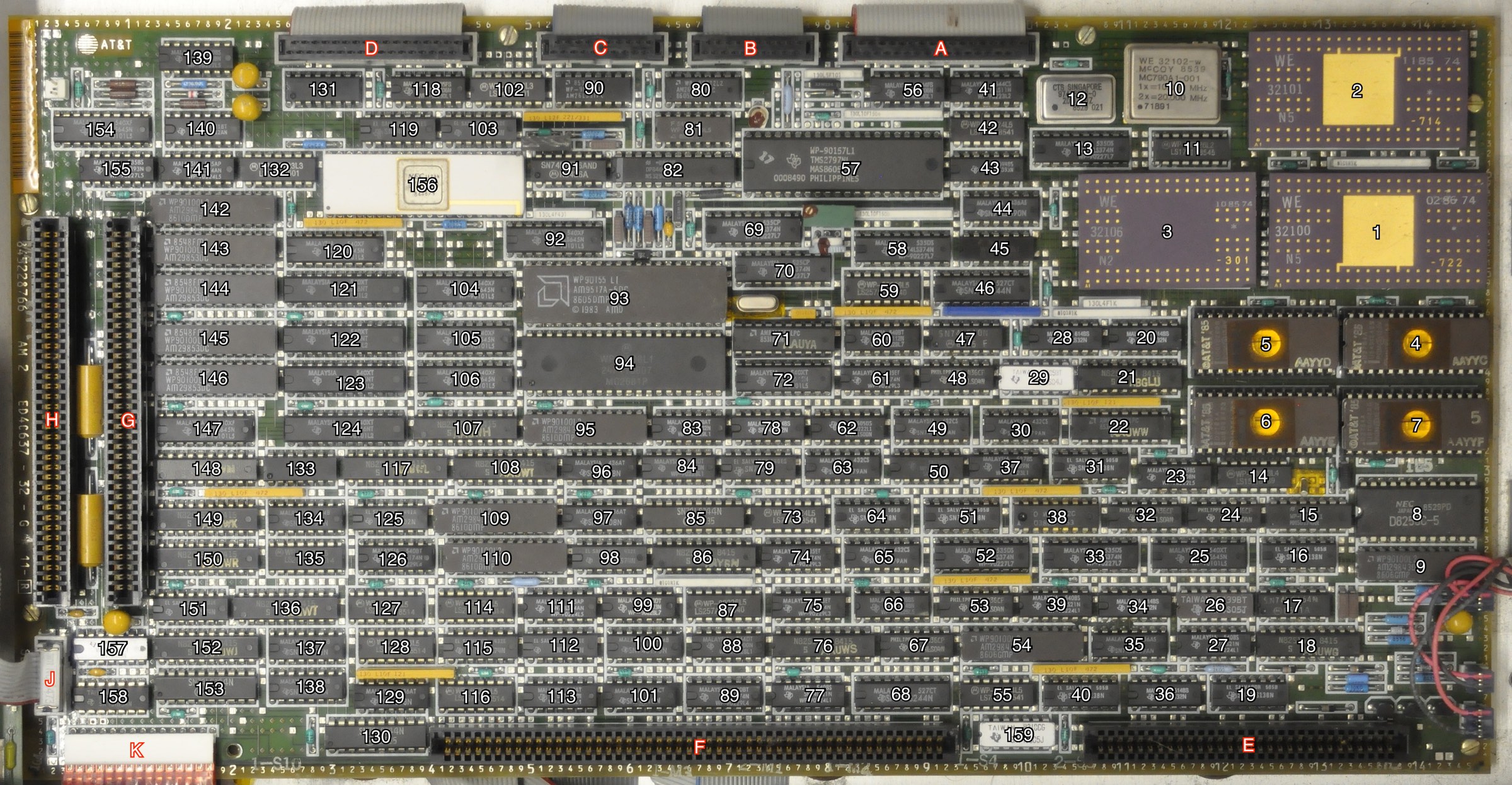
In this figure, numbers are somewhat arbitrarily ordered, but roughly from top to bottom, right to left.
| Number | Name | Purpose |
|---|---|---|
| 1 | WE32100 | CPU |
| 2 | WE32101 | MMU |
| 3 | WE32106 | Math Accelerator Unit |
| 10 | WE32102 | CPU clock source |
| 4,5,6,7 | i2764 | System ROM |
| 8 | 8253 | Interval timer interrupt source |
| 57 | TMS2797 | Floppy disk controller |
| 93 | AM9517A | Multimode DMA controller |
| 94 | 2681 | Dual UART and interval timer interrupt source |
| 156 | μDP7261 | Hard disk controller |
| A | Header | Floppy disk connector |
| B | Header | MFM hard disk data connector |
| C | Header | MFM hard disk data connector |
| D | Header | MFM hard disk control connector |
| E,F | Connector | Backplane card edge connector |
| G | Memory | Memory slot A (1MB,2MB) |
| H | Memory | Memory slot B (1MB,2MB) |
All Parts
| IC | Qty. | Description |
|---|---|---|
| 2681 | 1 | Dual UART |
| 26LS32 | 1 | Quad differential line receiver |
| 27LS31 | 1 | Quad differential line driver |
| 7406 | 2 | Hex inverter buffer drivers with O.C. outputs |
| 7407 | 2 | Hex buffer drivers with O.C. outputs |
| 74F04 | 1 | Hex inverters |
| 74F11 | 1 | Triple 3-input AND gates |
| 74LS00 | 1 | Quad 2-input NAND gates |
| 74LS02 | 1 | Quad 2-input NOR gates |
| 74LS04 | 5 | Hex inverters |
| 74LS05 | 1 | Hex inverters with O.C. outputs |
| 74LS08 | 2 | Quad 2-input AND gates |
| 74LS09 | 1 | Quad 2-input AND gates with O.C. outputs |
| 74LS10 | 1 | Triple 3-input NAND gates |
| 74LS11 | 1 | Triple 3-input AND gates |
| 74LS112 | 1 | Dual neg.-edge-triggered master/slave J-K flip-flops |
| 74LS125 | 1 | Quad bus buffers with tri-state outputs |
| 74LS126 | 1 | Quad bus buffers with tri-state outputs |
| 74LS138 | 6 | 3-to-8 line decoder/demux |
| 74LS139 | 1 | Dual 2-to4 decoder/demux |
| 74LS14 | 2 | Hex inverter with Schmitt trigger inputs |
| 74LS148 | 1 | 8-to-3 priority encoder |
| 74LS151 | 1 | 8-input multiplexer |
| 74LS157 | 1 | Quad 2-input multiplexers |
| 74LS164 | 1 | 8-bit serial-in/parallel-out shift reg. |
| 74LS174 | 1 | Hex D-type flip-flops |
| 74LS21 | 3 | Dual 4-input AND gates |
| 74LS244 | 5 | Non-inverting buffer/driver |
| 74LS257 | 7 | Quad 2-input multiplexers with tri-state outputs |
| 74LS279 | 4 | Quad SR Latches |
| 74LS32 | 5 | Quad 2-input OR gates |
| 74LS374 | 6 | Octal D-Type latches with tri-state outputs |
| 74LS390 | 1 | Dual decade counter |
| 74LS393 | 2 | Dual 4-state binary counter |
| 74LS645 | 9 | Octal bus transceiver |
| 74LS646 | 4 | Octal bus transceiver with tri-state output |
| 74LS74 | 5 | Dual D-type flip-flop |
| 74S00 | 2 | Quad 2-input NAND gates |
| 74S02 | 1 | Quad 2-input NOR gates |
| 74S03 | 1 | Quad 2-input NAND gates with O.C. outputs |
| 74S04 | 1 | Hex inverters |
| 74S05 | 1 | Hex inverters with O.C. outputs |
| 74S08 | 3 | Quad 2-input AND gates |
| 74S10 | 1 | Triple 3-input NAND gates |
| 74S112 | 1 | Dual neg.-edge-triggered master/slave J-K flip-flops |
| 74S174 | 2 | Hex D-type flip-flops |
| 74S175 | 4 | Quad D-type flip-flops |
| 74S32 | 2 | Quad 2-input OR gates |
| 74S74 | 8 | Dual D-Type positve edge triggered flip-flops |
| 75188 | 1 | Quad RS-232 line drivers |
| 75189 | 1 | Quad RS-232 line receivers |
| 82S153 | 12 | Field programmable logic array (PLA) |
| 974-6033-0 | 1 | 20 MHz xtal osc. |
| AM29843 | 5 | Bus interface latches |
| AM29853 | 5 | Parity bus transceiver |
| AM9517A | 1 | Multimode DMA controller |
| AMPAL16 | 2 | Programmable array logic (PAL) |
| D2764A | 4 | EPROM |
| D8253C | 1 | Programmable interval timer |
| DP8465 | 1 | PLL |
| MM58174A | 1 | Real time clock |
| TMS2797 | 1 | Floppy disk controller |
| μDP7261 | 1 | Hard disk controller |
| WE32100 | 1 | CPU |
| WE32101 | 1 | MMU |
| WE32102 | 1 | Bi-phase 10MHz xtal osc. |
| WE32106 | 1 | FPU/MAU |
| WE62C | 1 | Unknown (marked “O WE 62C”) |
| Total | 159 |
Notes
- The 12
82S153PLAs are marked: AAUWG, ABGLU, AAUWS, AAYBN, AAUWH, AAUWL, AAUWT, ABGWT, AAUWN, AAUWK, AAUWR, AAUWJ